GaN defect single photon emitters
In this work, we investigate single-photon defect emitters in HVPE grown GaN epitaxial layers. GaN defect emitters exhibit strong ZPLs in the 600–700 nm wavelength range at room temperature. Representative emission spectra of some SPEs are shown in Fig. 1a. The ZPL center wavelengths of emitters E1 through E5 are 602.9 nm, 628.7 nm, 650.1 nm, 684.5 nm and 710.5 nm, respectively. These wavelengths match well with the wavelengths for GaN SPEs reported earlier10.
(a) Representative PL spectra of five GaN SPEs, E1 through E5, are plotted at room temperature. (b) SEM image of five solid immersion lenses (SILs), each fabricated around a SPE, is shown. Each SIL is a hemisphere of radius 2.5 \(\upmu\)m. (c) The measured PL intensities of a SPE before and after the fabrication of a SIL are plotted as a function of the pump power. (d) The spatial PL map of a single emitter within a SIL is shown.
GaN is a high index material in the visible wavelength range. As a consequence, most PL is trapped inside the substrate due to total internal reflection. To increase the photon collection efficiency, a solid immersion lens (SIL)23,24 in the form of a hemisphere of radius 2.5 \(\upmu\)m was fabricated on top of each emitter by focused ion beam milling of GaN, as shown in Fig. 1b. To avoid deflection of the ion beam due to surface charge accumulation during milling, a 30 nm Al layer was sputtered on the GaN surface before milling and Al left after milling was removed using a wet etch. PL collection efficiency from the SPEs was found to be enhanced by factors in the 4–5 range (using a 0.9 NA objective). Figure 1c shows the PL intensity (in kcps) of an emitter before and after the fabrication of a SIL as a function of the pump power. Figure 1d shows the PL map of a defect emitter in the center of the SIL. The measured PL intensity \(I_{pl}\) can be fitted by the standard relation,
$$\begin{aligned} I_{pl} = I_{sat}\frac{P_{pump}}{P_{pump}+P_{sat}} \end{aligned}$$
(1)
Here, \(I_{sat}\) is the saturation PL intensity, \(P_{pump}\) is the pump power, and \(P_{sat}\) is the saturation pump power. For the data shown in Fig. 1c, \(P_{sat}\) is 650 \(\upmu\)W, \(I_{sat}\) is 171 kcps without the SIL and 779 kcps with the SIL, indicating that the PL collection efficiency is enhanced by a factor of \(\sim\) 4.5. This enhancement in light collection ensured a sufficient signal-to-noise ratio for cryogenic temperature measurements when a smaller NA (0.7) objective was used.

(a) The second order correlation function \(g^{(2)}(\tau )\) of emitter E3 is plotted. \(g^{(2)}(0)=0.17\). (b) \(g^{(2)}(\tau )\) of emitter E4 is plotted. \(g^{(2)}(0)=0.19\). The solid lines show the fits obtained using the expression given in the text.
In what follows, we focus mostly on two emitters, E3 and E4 in Fig. 1a, with center emission wavelengths 650.1 nm (\(\sim\) 1907.4 meV) and 684.5 nm (\(\sim\) 1811.5 meV), respectively. Most other emitters were found to exhibit characteristics similar to them. Figure 2 shows the measured second order correlation function \(g^{(2)}(\tau )\) for these two emitters at room temperature using a pump power of 50 \(\mu\)W. \(g^{(2)}(\tau )\) was obtained using the time-tagged time-resolved (TTTR) mode of the MultiHarp150 instrument and was properly normalized. For both emitters, \(g^{(2)}(\tau )\) can be fitted by the expression,
$$\begin{aligned} g^{(2)}(\tau )=1-ae^{-|\tau |/\tau _{1}}+be^{-|\tau |/\tau _{2}} \end{aligned}$$
(2)
The fits are shown by the solid lines in Fig. 2. The extracted values of \(\tau _{1}\) are \(3.18\pm 0.24\) ns and \(2.2\pm 0.17\) ns for emitters E3 and E4, respectively, and the values of \(\tau _{2}\) are \(74\pm 27\) ns and \(65\pm 33\) ns for emitters E3 and E4, respectively. \(g^{(2)}(0)\) equals 0.17 and 0.19 for emitters E3 and E4, respectively, which confirms these defects as single-photon emitters. The measured values of \(\tau _{1}\) and \(\tau _{2}\) are in good agreement with the values reported previously10.

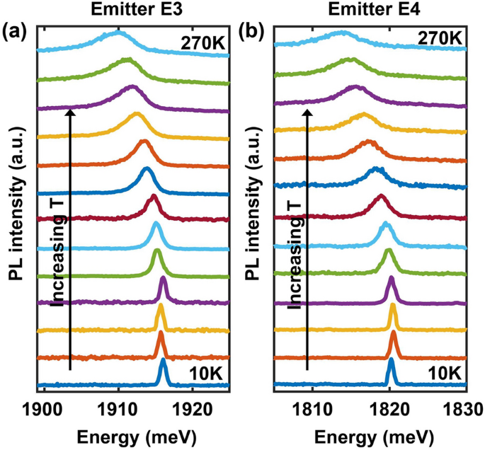
The emission spectra of emitter E3 (a) and E4 (b) are plotted for different temperatures in the 10–270 K range (with an increment of 20 K).
Temperature dependence of the ZPL emission spectra

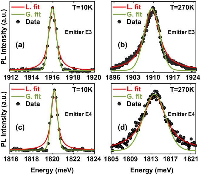
The ZPL spectra with a Gaussian and a Lorentzian fits at 10 K (a) and 270 K (b) for emitter E3 are plotted. Also shown are the ZPL spectra with a Gaussian and Lorentzian fits at 10 K (c) and 270 K (d) for emitter E4.

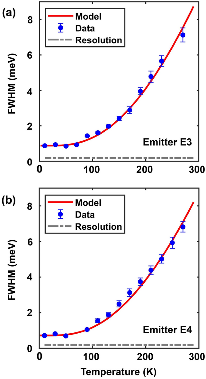
The FWHM linewidths of emitter E3 (a) and emitter E4 (b) are plotted as a function of the temperature. The solid lines are the fit to the data using the theoretical model discussed in the text.
The ZPL emission spectra were measured for temperatures in the 10–270 K range and the results are shown in Fig. 3 for emitters E3 and E4. Other emitters display similar trends. The center emission energies are seen to redshift with an increase in the temperature. The ZPL energy of E3 shifts from 1916 meV at 10 K to 1909.4 meV at 270 K. In the case of E4, the ZPL energy shifts from 1820.2 meV at 10 K to 1813.5 meV at 270 K. We don’t observe a S-shaped temperature dependence of the ZPL center energies reported previously10.
We look at the spectral shape of the ZPL as a function of the temperature. Our data shows that the ZPL spectra evolve from a Gaussian lineshape at temperatures below \(\sim\)50 K to a Lorentzian lineshape at temperatures above \(\sim\)125 K. This is shown in detail in Fig. 4 which plots the ZPL spectra of emitters E3 and E4 at low (10 K) and high (270 K) temperatures, along with Gaussian and Lorentzian fits to these spectra at the two temperatures. The data shown was obtained using a pump power of 300 \(\mu\)W. At 10 K, the spectrum of E3 (E4) can be fit much better with a Gaussian spectral function with a full-width-half-maximum (FWHM) linewidth of 0.88 meV (0.72 meV). Whereas at 270 K, the spectrum of E3 (E4) can be fit much better with a Lorentzian spectral function with a FWHM linewidth of 7.12 meV (6.82 meV). These observations suggest that two different mechanisms are contributing to the linewidth. One may make the simplest assumption that these two mechanisms are independent. Under this assumption, the ZPL spectral shape is more accurately given by a Voigt function \(V(\omega ;\sigma ,\gamma )\) which is a convolution of Gaussian and Lorentzian functions14,22,25,
$$\begin{aligned} V(\omega ;\sigma ,\gamma ) \propto \int _{-\infty }^{+\infty }G(\omega ^{‘};\sigma )L(\omega -\omega ^{‘};\gamma )d\omega ^{‘} \end{aligned}$$
(3)
Here, \(G(\omega ;\sigma )\) and \(L(\omega ;\gamma )\) are Gaussian and Lorentzian functions with FWHM equal to \(f_{G} = 2\sigma \sqrt{2\ln 2}\) and \(f_{L} = 2\gamma\), respectively. The FWHM \(f_{V}\) of the Voigt function can be written as,
$$\begin{aligned} f_V=0.5346f_L+\sqrt{0.2166 f_{L}^{2}+f_{G}^{2}} \end{aligned}$$
(4)
By fitting the measured ZPL spectra with a Voigt function, the temperature dependent FWHM of its Gaussian and Lorentzian components can be extracted. We find that the FWHM \(f_{G}\) of the Gaussian component is temperature independent and is around 0.88 meV (0.72 meV) for E3 (E4). An emission spectrum with a temperature independent FWHM and a Gaussian lineshape is a common signature of spectral diffusion whereby the emitter emission energy changes in time as a result of factors such as changes in the electrical environment of the emitter. To gain insight into the mechanism responsible for the Lorentzian component, which dominates at temperatures higher than \(\sim\)125 K, we look at the FWHM linewidth of the ZPL as a function of the temperature. This data is shown in Fig. 5a for emitter E3 and in Fig. 5b for emitter E4. It is clear that the Lorentzian component dominates the ZPL linewidth at temperatures higher than \(\sim\)125 K. Using the expression given in Eq. (4), we find that the temperature dependence of the FWHM of the Lorentzian component cannot be adequately fitted with an expression proportional to \(T^{n}\), where n is any integer greater than or equal to 3 (n equals 3, 5, and 7 for some common dephasing mechanisms mentioned earlier in this paper). Figure S1 in the supplementary information shows the poor comparison with the data that is obtained if the temperature dependence of the linewidth of the Lorentzian component is assumed to be \(T^{3}\). This indicates that the common dephasing mechanisms, discussed earlier in this paper, might not be the dominant dephasing mechanisms in the case of GaN SPEs. Given that the measured ZPL linewidths for GaN SPEs, shown in Fig. 5, are orders of magnitude larger than the linewidths that would result from relaxation processes (as estimated by the measured \(g^{(2)}\) function), the dephasing mechanism is quite strong. Below, we present a theoretical model for dephasing and show that this model fits the data very well.
A theoretical model for dephasing in GaN single-photon emitters
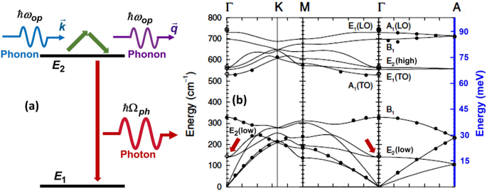
The dephasing mechanism proposed here is depicted in Fig. 6a and it involves absorption/emission of optical phonons in an elastic Raman process which results in the scattering of an optical phonon from the defect. In other words, dephasing of the electron state in the defect occurs by the elastic scattering of thermally excited optical phonons from the electron. A similar mechanism involving acoustic phonons is known to result in a dephasing rate proportional to \(T^{7}\) in solid state emitters19,20. Although as depicted in Fig. 6a the dephasing occurs in only the excited state, dephasing occurring by a similar process in the ground state can be handled in a way similar to the one shown below.
We assume that the Hamiltonian for the defect state interacting with optical phonons is,
$$\begin{aligned}&H = \sum _{j} \left[ E_{j} + \alpha _{j} F(t) \right] c_{j}^{\dagger }c_{j} \nonumber \\&\qquad + \frac{1}{\sqrt{V}} \sum _{j \ne 2,\mathbf {k}} \left( M_{j,\mathbf {k}}c_{j}^{\dagger }c_{2} + M^{*}_{j,-\mathbf {k}}c_{2}^{\dagger }c_{j}\right) \left( a_{\mathbf {k}} + a_{-\mathbf {k}}^{\dagger }\right) \nonumber \\&\qquad + \frac{1}{\sqrt{V’}} \sum _{\mathbf {k}} \left( F_{\mathbf {k}}c_{1}^{\dagger }c_{2} + F^{*}_{-\mathbf {k}}c_{2}^{\dagger }c_{1}\right) \left( b_{\mathbf {k}} + b_{-\mathbf {k}}^{\dagger }\right) \nonumber \\&\qquad + \sum _{\mathbf {k}} \hbar \omega _{\mathbf {k}} a_{\mathbf {k}}^{\dagger }a_{\mathbf {k}} + \sum _{\mathbf {k}} \hbar \Omega _{\mathbf {k}} b_{\mathbf {k}}^{\dagger }b_{\mathbf {k}} \end{aligned}$$
(5)
Here, \(c_{j}\), \(a_{\mathbf {k}}\), and \(b_{\mathbf {k}}\) are the destruction operators for the electron, optical phonon, and photon states, respectively. \(E_{j}\) are the energies of the emitter electron states and, as shown in Fig. 6, \(j=1,2\) states participate in photon emission. \(\omega _{\mathbf {k}}\) are the frequencies of the optical phonons in a band that is coupled to the emitter. \(\Omega _{\mathbf {k}}\) are the frequencies of the photon modes. V (\(V’\)) is the volume in which the phonon (photon) modes are normalized. The coupling parameters \(M_{j,\mathbf {k}}\) in the electron-optical phonon interaction Hamiltonian describe deformation potential interaction between the defect electron and the optical phonons. The coupling terms \(F_{\mathbf {k}}\) describe the coupling between the emitter dipole and the radiation field. To model spectral diffusion, we have included terms in the electron energies linear in the external time-dependent electric field F(t) which is assumed to be caused by time-dependent charges in the environment. Terms quadratic in F(t) can also be included in the Hamiltonian but their inclusion does not affect the discussion that follows and the conclusions26. We assume that \(\langle F(t) \rangle = 0\) and \(\langle F(t) F(t’)\rangle = F_{o}^{2} e^{-\lambda |t-t’|}\), where \(\lambda ^{-1}\) is the field correlation time and will be assumed to be much longer than any other time scale in the problem. The electron-phonon interaction term in the Hamiltonian couples the emitter excited state to virtual states that can be eliminated (as discussed in the Supplementary Information Section) to give the following effective Hamiltonian for the elastic phonon scattering process shown in Fig. 6a.

(a) Proposed mechanism for dephasing involving absorption/emission of optical phonons via an elastic Raman process. \(E_{2}\) (\(E_{1}\)) represents the excited (ground) state energy of the emitter. (b) Phonon bands in wurtzite GaN are reproduced from the work of Ruf et al.27. The energy of the \(E_{2}(low)\) optical phonon mode at the zone center matches the value obtained by fitting the model to the data.
$$\begin{aligned} H^{eff}_{e-ph} = c_{2}^{\dagger }c_{2} \frac{1}{V} \sum _{\mathbf {k} \ne \mathbf {q}} G_{\mathbf {k},\mathbf {q}} a_{\mathbf {q}}^{\dagger } a_{\mathbf {k}} \end{aligned}$$
(6)
where,
$$\begin{aligned} G_{\mathbf {k},\mathbf {q}} = \sum _{j \ne 2} \left[ \frac{M^{*}_{j,\mathbf {q}}M_{j,\mathbf {k}}}{E_{2}-E_{j} + \hbar \omega _{\mathbf {k}}} + \frac{M^{*}_{j,-\mathbf {k}}M_{j,-\mathbf {q}}}{E_{2}-E_{j} – \hbar \omega _{\mathbf {q}}} \right] \end{aligned}$$
(7)
If the electron-phonon interaction is via optical deformation potential then it is reasonable to assume that \(G_{\mathbf {k},\mathbf {q}}\) will be large only when both \(\mathbf {k},\mathbf {q}\) are small (near the center of the Brillouin zone)28. The ZPL emission spectrum \(S(\omega )\) can be obtained from the relation29,
$$\begin{aligned} S(\omega )= & {} \int dt \, e^{-i\omega t} \langle \sigma _{+}(t) \sigma _{-}(0) \rangle / \langle c_{2}^{\dagger }c_{2} \rangle \nonumber \\= & {} \int dt \, e^{-i\omega t} \langle c_{2}^{\dagger }(t) c_{1}(t) c_{1}^{\dagger }c_{2} \rangle /\langle c_{2}^{\dagger }c_{2} \rangle \end{aligned}$$
(8)
Using the cumulant expansion technique for the quantum propagator16,30, the above expression gives,
$$\begin{aligned} S(\omega ) \approx \int dt \, e^{-i\left[ \omega – (E_{2}-E_{1})/\hbar \right] t} \, e^{-\sigma ^{2}t^{2}/2} e^{-(\gamma + \gamma _{sp}) |t|} \end{aligned}$$
(9)
Here, \(\sigma = |\alpha _{2}-\alpha _{1}|F_{o}/\hbar\), \(2\gamma _{sp}\) is the spontaneous photon emission rate, and the dephasing rate \(\gamma\) due to interaction with phonons is,
$$\begin{aligned} \gamma= & {} \frac{2\pi }{\hbar ^{2}} \int d\omega D^{2}(\omega ) |G(\omega )|^{2} \, n(\omega )\left[ n(\omega ) + 1 \right] \nonumber \\\approx & {} \frac{2\pi }{\hbar ^{2}} n(\omega _{op})\left[ n(\omega _{op}) + 1 \right] \int d\omega D^{2}(\omega ) |G(\omega )|^{2} \end{aligned}$$
(10)
\(n(\omega )\) is the thermal boson occupation factor and \(D(\omega )\) is the density of states function for the optical phonons. In the writing the result in Eq. (9), we have ignored constant shifts in the energy \(E_{2}\) that result from phonon and photon interactions. We will assume that \(\gamma>> \gamma _{sp}\) and that the dephasing is almost entirely due to interaction with phonons. The product \(D^{2}(\omega ) |G(\omega )|^{2}\) inside the integral is assumed to be peaked near the frequency \(\omega _{op}\), which is the frequency of the optical phonon mode coupled to the defect. Eq. (9) shows that the ZPL spectral shape will be given by a Voigt function. The expression for \(\gamma\) shows that the temperature dependence of the dephasing rate is determined by the product \(n(\omega _{op})\left[ n(\omega _{op}) + 1 \right]\), which gives a temperature dependence very different from any power law.
Using the expression for the FWHM of \(S(\omega )\) given earlier in Eq. (4) with the experimentally determined values of the Gaussian component \(f_{G}\), and using the temperature dependence of \(\gamma\) given by the expression in Eq. (10) for the Lorentzian component \(f_{L}=2\gamma\), we can fit the measured FWHM of the ZPL, for both emitters E3 and E4, over the entire 10–270 K temperature range with a root mean square error less than 0.05 meV provided we assume that \(\hbar \omega _{op}\) equals 19 meV ± 0.5 meV. The fits obtained for \(\hbar \omega _{op} = 19\) meV are shown by the solid lines in Fig. 5. The excellent agreement between the data and the model begs the question if 19 meV is close to any one of the bulk optical phonons energies in GaN. Quite remarkably, the lowest energy Raman-active \(E_{2}(low)\) optical phonon band in GaN has energy equal to \(\sim\)18 meV at the \(\Gamma\)-point of the Brillouin zone, as shown in Fig. 6b27. Since, as stated earlier, \(|G(\omega )|^{2}\) is expected to be large near the zone center, the experimental value of 19 meV for \(\hbar \omega _{op}\) is reasonable and consistent with dephasing being caused by the coupling between the emitter and the bulk \(E_{2}(low)\) optical phonons. The \(E_{2}(low)\) optical phonon in GaN is known to be Raman active and couples strongly to the electronic states in the valence and conduction bands31.


 Bitcoin
  Ethereum
  Tether
  XRP
XRP  Solana
  USDC
USDC  Lido Staked Ether
  Dogecoin
  TRON
TRON  Cardano
  Wrapped stETH
  Wrapped Bitcoin
  Chainlink
  Ethena USDe
  Hyperliquid
  Sui
Sui  Figure Heloc
  Stellar
  Avalanche
  Wrapped eETH
  Bitcoin Cash
  WETH
WETH  Hedera
  Litecoin
  LEO Token
  Coinbase Wrapped BTC
  Binance Bridged USDT (BNB Smart Chain)
  USDS
USDS  Shiba Inu
  Cronos
  Toncoin
  Mantle
  USDT0
USDT0  WhiteBIT Coin
  Polkadot
  Monero
  Ethena Staked USDe
  World Liberty Financial
  Uniswap
  OKB
OKB  Dai
Dai  Aave
Aave  Ethena
  Pepe
Pepe  Bitget Token
  Aptos
Aptos  NEAR Protocol
  Jito Staked SOL